Nano Vanadium Dioxide Materials: A Comprehensive Guide to Monoclinic Particles, W-Doped, and Nanowires
Vanadium dioxide (VO₂) has emerged as one of the most promising thermochromic materials for next-generation energy-efficient technologies. When engineered at the nanoscale, VO₂ unlocks extraordinary properties that bulk materials simply cannot match. This guide examines three critical nano-VO₂ materials—pure phase Monoclinic VO2 nanoparticles, tungsten-doped VO2 nanoparticles, and VO2 nanowires—providing researchers and engineers with actionable insights for material selection and application development.
---
Understanding the Foundation: Why Nano-VO₂ Matters
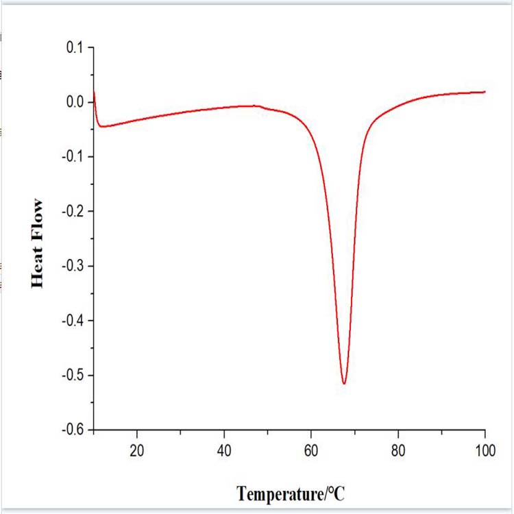
At approximately 68°C, bulk VO₂ undergoes a reversible first-order metal-insulator transition (MIT), accompanied by dramatic changes in optical and electrical properties. This phase transition, driven by the Mott-Hubbard mechanism, transforms VO₂ from a monoclinic semiconductor to a rutile metallic state. However, bulk VO₂ suffers from high transition temperatures, poor visible transmittance, and limited solar modulation efficiency.
Nanostructuring addresses these limitations through three primary mechanisms: quantum confinement effects that shift optical absorption, increased surface-area-to-volume ratios that enhance reaction kinetics, and dopant incorporation flexibility that enables precise phase-transition engineering. These advantages make nano-VO₂ indispensable for smart windows, thermal sensors, energy storage systems, and neuromorphic computing devices.
---
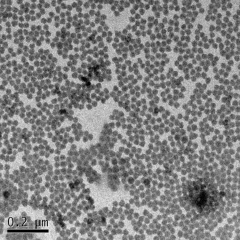
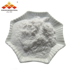
Nano VO₂ Particles: Versatile Building Blocks
Nano VO₂ particles (typically 100–200 nm) represent the most commercially accessible form of nanostructured vanadium dioxide. Their quasi-spherical morphology enables homogeneous dispersion in polymer matrices, paints, and coatings.
Key Performance Parameters:
- Phase transition temperature: 67°C ± 3°C
The principal limitation of undoped nano-VO₂ particles lies in their high transition temperature, which restricts practical deployment in ambient-temperature applications such as architectural glazing.
---
W-Doped Nano VO₂: Engineering the Phase Transition
Tungsten doping represents the most effective strategy for depressing VO₂'s phase transition temperature toward room-temperature operation. Each atomic percent of tungsten incorporation typically reduces the transition temperature by approximately 20–26°C, enabling precise calibration for target applications.
Critical Doping Considerations:
Tungsten Content (at%)
|
Transition Temperature (°C)
|
Primary Application
|
|
0%
|
67°C ± 3°C
|
High-temperature sensors
|
|
1%
|
45°C ± 3°C
|
Industrial thermal switches
|
|
1.5%
|
33°C ± 3°C
|
Automotive smart glazing
|
|
2%
|
22°C ± 3°C
|
Building energy-efficient windows
|
W-doped nano-VO₂ maintains the monoclinic-rutile structural transition while introducing localized electronic states that facilitate carrier nucleation at lower thermal energies. However, excessive tungsten content (>3 at%) degrades solar modulation efficiency and reduces crystallinity, establishing a practical doping ceiling for most optical applications.
For smart window applications, W-doped nano-VO₂ particles embedded in polyethylene terephthalate (PET) or polyvinyl butyral (PVB) interlayers demonstrate solar modulation exceeding 15% while maintaining visible transmittance above 45%—meeting the performance thresholds for commercial building integration.
---
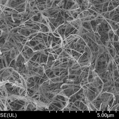
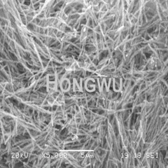
VO₂ Nanowires: One-Dimensional Functional Architectures
VO₂ nanowires exhibit unique anisotropic properties stemming from their high aspect ratios (length: 10um; diameter:100 nm). These one-dimensional structures demonstrate orientation-dependent optical switching, enhanced electron transport along the wire axis, and superior mechanical flexibility compared to particulate counterparts.
Distinctive Characteristics:
- Anisotropic phase transition: Nanowires often exhibit broadened transition regions due to surface-stabilized metastable phases
- Enhanced local field effects: Subwavelength diameters enable plasmonic interactions in the metallic phase
- Direct device integration: Individual nanowires serve as active elements in field-effect transistors, memristors, and single-nanowire sensors
Recent research published in Advanced Functional Materials (2025) demonstrated that VO₂ nanowire arrays grown on flexible substrates achieve reversible resistance switching ratios exceeding 10⁴, positioning them as promising candidates for non-volatile memory and artificial synapse applications in neuromorphic computing architectures.
---
Comparative Selection Guide
Property
|
monoclinic VO2
|
W Doped VO2
|
Nanowires
|
Transition Temp
|
68°C
|
Tunable (10–50°C)
|
50–65°C (size-dependent)
|
Solar Modulation
|
Moderate
|
High
|
Variable (anisotropic)
|
Dispersibility
|
Excellent
|
Excellent
|
Challenging
|
Scalability
|
High
|
Moderate
|
Moderate
|
Best Application
|
Coatings, Composites
|
Smart windows
|
Sensors,Eelectronics
|
Cost Level
|
$
|
$$
|
$$$
|
---
Frequently Asked Questions
Q: Can W-doped nano-VO₂ achieve room-temperature switching without sacrificing optical performance?
A: At 2.0 at% tungsten doping, transition temperatures approach 20°C with acceptable solar modulation (ΔTsol 12–14%). However, visible transmittance decreases, necessitating anti-reflection coatings or optimized particle distributions for commercial window applications.
Q: Are VO₂ nanowires commercially available?
A: Currently, VO₂ nanowires remain primarily a research material supplied by specialized nanomaterial vendors in gram quantities. Industrial-scale production remains limited by growth throughput and substrate costs.
---
The nano-VO₂ landscape is evolving rapidly. For organizations evaluating nano-VO₂ adoption, W-doped nanoparticles offer the most immediate commercial pathway for energy-efficient glazing, while nanowires present high-value opportunities in next-generation electronics. Understanding the distinct advantages and limitations of each morphology enables informed material selection aligned with specific performance requirements and manufacturing constraints.


 日本語
日本語 English
 français
 Deutsch
 русский
 italiano
 español
 português
 한국의
한국의 Türkçe


 8620-87226359,8620-87748917
